home add to favorite
Email: info@creative-nanotech.com
 
Your position - Carbon Nanotubes
  Creative-Nano
  Carbon Nanotubes
  Nano Metal Powder
  Nano Compound Powder
  Contact Us
Email:
info@creative-nanotech.com
 
  Carbon Nanotubes

Product description
- Single wall carbon nanotubes (SWNTs)

Purity: >90%
OD: 1-2nm [OD=Outside Diameter]
ID: 0.8-1.6nm [ID=Inside Diameter]
Length: 5-30um
SSA: >380m2/g [SSA=Special Surface Area]
Color: Black
Bulk density: 0.14 g/cm3
True density: ~2.1 g/cm3
EC:>100s/cm [EC=Electric Conductivity]
Making method: CVD

Figure 1. A TEM image of our SWNTs 90wt% 1-2nm OD, CNTs

- Double wall carbon nanotubes (DWNT)

Purity: >60%
OD: 2-4nm [OD=Outside Diameter]
ID: 1-2nm [ID=Inside Diameter]
Length: ~50um
SSA: >350m2/g [SSA=Special Surface Area]
Color: Black
True density: ~2.1 g/cm3
EC:>100s/cm [EC=Electric Conductivity]
Making method: CVD

Figure 2. A SEM image of our SWNTs 90wt% 1-2nm OD, CNTs.
- Multi wall carbon nanotubes (MWCNT)

<8nm, 95+%, MWCNT

Purity: >95%                 
OD: <8nm   [OD=Outside Diameter]
ID: 2-5nm   [ID=Inside Diameter]
Length: 10-30um
SSA: >500m2/g    [SSA=Special Surface Area]
Color: Black
Bulk density: 0.27 g/cm3
True density: ~2.1 g/cm3
EC:>100s/cm [EC=Electric Conductivity]
Making method: CVD

Figure 3. Scanning Electron Microscopy (SEM).
8-15nm, 95+%, MWCNT

Purity: >95%
OD: 8-15nm [OD=Outer Diameter]
ID: 3-5nm [ID=Inner Diameter]
Length: ~50um
SSA: >233m2/g [SSA=Special Surface Area]
Color: Black
Bulk density: 0.15 g/cm3
True density: ~2.1 g/cm3
EC:>100s/cm [EC=Electric Conductivity]
Making method: CVD

Figure 4. Scanning Electron Microscopy (SEM)
10-20nm, 95+%, MWCNT

Purity: >95%
OD: 10-20nm [OD=Outer Diameter]
ID: 5-10nm [ID=Inner Diameter]
Length: 10-30um
SSA: >200m2/g [SSA=Special Surface Area]
Color: Black
Bulk density: 0.22 g/cm3
True density: ~2.1 g/cm3
EC:>100s/cm [EC=Electric Conductivity]
Making method: CVD

Figure 5. Scanning Electron Microscopy (SEM) 
20-30nm, 95+%, MWCNT

Purity: >95%
OD: 20-30nm [OD=Outer Diameter]
ID: 5-10nm [ID=Inner Diameter]
Length: 10-30um
SSA: >110m2/g [SSA=Special Surface Area]
Color: Black
Bulk density: 0.28g/cm3
True density: ~2.1 g/cm3
EC:>100s/cm [EC=Electric Conductivity]
Making method: CVD

Figure 6. Scanning Electron Microscopy (SEM)
30-50nm, 95+%, MWCNT

Purity: >95%
OD: 30-50nm [OD=Outer Diameter]
ID: 5-12nm [ID=Inner Diameter]
Length: 10-20um
SSA: >60m2/g [SSA=Special Surface Area]
Color: Black
Bulk density: 0.22 g/cm3
True density: ~2.1 g/cm3
EC:>100s/cm [EC=Electric Conductivity]
Making method: CVD

Figure 7. Scanning Electron Microscopy (SEM)
>50nm, 95+%, MWCNT

>50nm, 95+%, MWCNTPurity: >95%
OD: >50nm [OD=Outer Diameter]
ID: 5-15nm [ID=Inner Diameter]
Length: 10-20um
SSA: >40m2/g [SSA=Special Surface Area]
Color: Black
Bulk density: 0.18 g/cm3
True density: ~2.1 g/cm3
EC:>100s/cm [EC=Electric Conductivity]
Making method: CVD

Figure 8. Scanning Electron Microscopy (SEM)

Benefits
▲ CVD Fabrication means high purity, low cost
▲ Available in metric ton quantities
▲ Suitable for a wide variety of applications


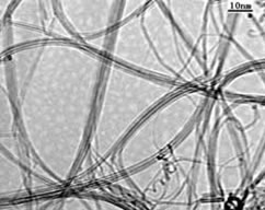
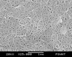
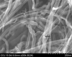
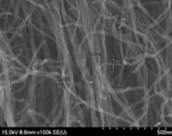
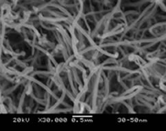
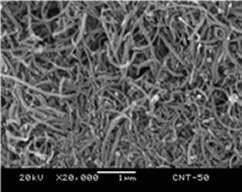
Nanotube Applications

SWCNTs are 100 times stronger than steel at one-sixth its weight. This makes them potentially highly valued as a means to strengthen composite materials. They also can be either very effective electrical conductors or semiconductors. Potential applications of nanotubes can be divided as follows:

▲ Actuators Conversion of electrical energy to mechanical energy and vice versa. Potential use in robotics, optical fiber switches and displays, prosthetic devices, etc.

▲ Sensors Correlations between adsorption of gases such as oxygen and conductance and thermoelectric power have been observed.

▲ Composites, Paints & Coatings Employing nanotubes as additive to polymer composites can give improved strength performance, thermal and electric conductivity. The challenge of anchoring nanotubes to polymeric structures has been addressed by functionalizing nanotube walls.

▲Biological Due to their physical dimensions similar to that of biologically active macromolecules such as proteins, and DNA, carbon nanotubes are finding increasing utility in biology related applications including sensors, drug delivery, enzyme immobilization, cancer research and DNA transfection.

▲ Electronics Depending on structural characteristics, carbon nanotubes are conducting or semi-conducting. Sizes of transistors and logic devices can be reduced significantly, e.g., logic devices made of a single nanotube with a transition between chiralities along its length. Others include: highly-ordered carbon nanotube arrays for data storage, displays, sensors & smaller computing devices. As SWCNTs can be clear, they open up the door for clear conducting polymers, and a replacement for Indium-Tin-Oxide.


  Copyright © [ Creative-Nano ] All Rights Reserved
  info@creative-nanotech.com ©